- 您现在的位置:买卖IC网 > Sheet目录508 > SI1902DL-T1-GE3 (Vishay Siliconix)MOSFET N-CH G-S 20V DUAL SC-70-6
Si1902DL
Vishay Siliconix
Dual N-Channel 20 V (D-S) MOSFET
FEATURES
PRODUCT SUMMARY
V DS (V) R DS(on) ( ? )
I D (A)
? Halogen-free According to IEC 61249-2-21
Definition
20
0.385 at V GS = 4.5 V
0.630 at V GS = 2.5 V
0.70
0.54
? TrenchFET ? Power MOSFETs: 2.5 V Rated
? 100 % R g Tested
? Compliant to RoHS Directive 2002/95/EC
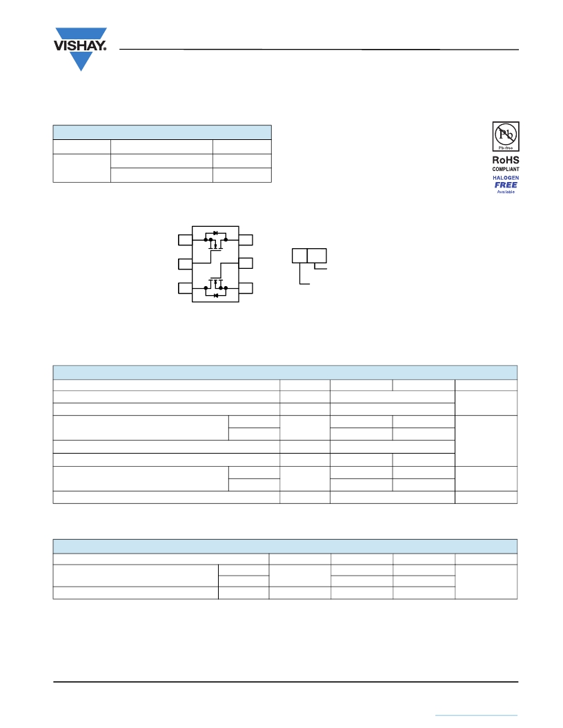
SOT-363
SC-70 (6-LEADS)
S 1
1
6
D 1
g
Marking in Code o d e
P PA A X
G 1
2
5
G 2
Lot Traceability
and Date Code
D 2
3
4
S 2
Part # Code
Top V iew
Ordering Information: Si1902DL-T1-E3 (Lead (Pb)-free with Tape and Reel)
Si1902DL-T1-GE3 (Lead (Pb)-free and Halogen-free)
ABSOLUTE MAXIMUM RATINGS (T A = 25 °C, unless otherwise noted)
Parameter
Drain-Source Voltage
Gate-Source Voltage
Symbol
V DS
V GS
5s
20
±12
Steady State
Unit
V
Continuous Drain Current (T J = 150 °C) a
Pulsed Drain Current
T A = 25 °C
T A = 85 °C
I D
I DM
0.70
0.50
1
0.66
0.48
A
Continuous Source Current (Diode Conduction) a
I S
0.25
0.23
Maximum Power Dissipation a
Operating Junction and Storage Temperature Range
T A = 25 °C
T A = 85 °C
P D
T J , T stg
0.30
0.16
- 55 to 150
0.27
0.14
W
°C
THERMAL RESISTANCE RATINGS
Parameter
Symbol
Typical
Maximum
Unit
Maximum Junction-to-Ambient a
Maximum Junction-to-Foot (Drain)
t ?? 5 s
Steady State
Steady State
R thJA
R thJF
360
400
300
415
460
350
°C/W
Notes:
a. Surface Mounted on 1" x 1" FR4 board.
Document Number: 71080
S11-2043-Rev. J, 17-Oct-11
www.vishay.com
1
This document is subject to change without notice.
THE PRODUCTS DESCRIBED HEREIN AND THIS DOCUMENT ARE SUBJECT TO SPECIFIC DISCLAIMERS, SET FORTH AT www.vishay.com/doc?91000
发布紧急采购,3分钟左右您将得到回复。
相关PDF资料
SI1926DL-T1-E3
MOSF N CH DUAL D-S 60V SC-70-6
SI1967DH-T1-E3
MOSFET 2P-CH 20V 1.3A SC70-6
SI1970DH-T1-GE3
MOSFET N-CH DUAL 30V SC70-6
SI2300DS-T1-GE3
MOSFET N-CH 30V SOT-23
SI2302CDS-T1-GE3
MOSFET N-CH 20V 2.6A SOT23-3
SI2303BDS-T1-GE3
MOSFET P-CH 30V 1.49A SOT23-3
SI2304BDS-T1-GE3
MOSFET N-CH 30V 2.6A SOT23-3
SI2304DDS-T1-GE3
MOSFET N-CH 30V 3.6A SOT23
相关代理商/技术参数
SI1902DL-T3
制造商:Vishay Intertechnologies 功能描述:Trans MOSFET N-CH 20V 0.66A 6-Pin SC-70 T/R
SI1903DL
制造商:VISHAY 制造商全称:Vishay Siliconix 功能描述:Dual P-Channel 2.5-V (G-S) MOSFET
SI1903DL_08
制造商:VISHAY 制造商全称:Vishay Siliconix 功能描述:Dual P-Channel 2.5-V (G-S) MOSFET
SI1903DL-T1
功能描述:MOSFET 20V 0.44A RoHS:否 制造商:STMicroelectronics 晶体管极性:N-Channel 汲极/源极击穿电压:650 V 闸/源击穿电压:25 V 漏极连续电流:130 A 电阻汲极/源极 RDS(导通):0.014 Ohms 配置:Single 最大工作温度: 安装风格:Through Hole 封装 / 箱体:Max247 封装:Tube
SI1903DL-T1-E3
功能描述:MOSFET 20V 0.44A RoHS:否 制造商:STMicroelectronics 晶体管极性:N-Channel 汲极/源极击穿电压:650 V 闸/源击穿电压:25 V 漏极连续电流:130 A 电阻汲极/源极 RDS(导通):0.014 Ohms 配置:Single 最大工作温度: 安装风格:Through Hole 封装 / 箱体:Max247 封装:Tube
SI1903DL-T1-E3
制造商:Vishay Siliconix 功能描述:MOSFET
SI1903DL-T1-GE3
功能描述:MOSFET 2P-CH 20V 410MA SC70-6 RoHS:是 类别:分离式半导体产品 >> FET - 阵列 系列:TrenchFET® 产品目录绘图:8-SOIC Mosfet Package 标准包装:1 系列:- FET 型:2 个 N 沟道(双) FET 特点:逻辑电平门 漏极至源极电压(Vdss):60V 电流 - 连续漏极(Id) @ 25° C:3A 开态Rds(最大)@ Id, Vgs @ 25° C:75 毫欧 @ 4.6A,10V Id 时的 Vgs(th)(最大):3V @ 250µA 闸电荷(Qg) @ Vgs:20nC @ 10V 输入电容 (Ciss) @ Vds:- 功率 - 最大:1.4W 安装类型:表面贴装 封装/外壳:PowerPAK? SO-8 供应商设备封装:PowerPAK? SO-8 包装:Digi-Reel® 产品目录页面:1664 (CN2011-ZH PDF) 其它名称:SI7948DP-T1-GE3DKR
SI1904EDH
制造商:VISHAY 制造商全称:Vishay Siliconix 功能描述:DUAL N-CHANNEL 25-V (D-S) MOSFET
